Time To ARM RTOS
Switching to ARM + K64F Bring-Up
My actual goal from day one was writing an RTOS, not a desktop kernel. x86 was where I learned the fundamentals — boot, GDT, IDT, serial — but RTOS work means microcontrollers, and microcontrollers mean ARM Cortex-M.
This post covers two things: the ARMv7-M system memory map (which I had to actually understand before touching the NVIC or writing a context switch), and the full K64F bare-metal bring-up — boot infrastructure, watchdog, UART, SysTick, PIT, GPIO, and all the painful problems along the way.
Plan: write in C first, port to Zig later. Project: github.com/hrasityilmaz/TamgaOs
Warning from experience: I wrote my own minimal linker script from zero — which is dangerous. One mistake and the chip goes sideways. If you decide to do the same: read the watchdog and memory-protection sections of your board's datasheet before writing a single line. That lesson cost me a week and three boards.
Why I'm switching to ARM
My goal is to build my own RTOS from scratch and fly my drone with it. Before ı experienced XFLR5 also to desing planes so ı hope everytihng will be amazingggg. And this posts also looks like some mixed but it is a devlog about me :)
INFO While reading this post, I noticed that some topics seem a little disconnected at first. I believe they'll make much more sense in the upcoming sections once we start diving deeper into the details. And ı downt want this part will be soo long but trust me will be more clear :)
Lastly after my last post already 2 weeks still ı am reading and reading plus -trust me- so long time ago ı strted to read and take notes but still continue ı guess this parts cmae ome rarely ı mean every 2 weeks looks like but of course on my plan ı will finish my TamgaOS.
Parts 1 through 3 of TamgaOS were x86 — booting in real mode, setting up the GDT and IDT, getting serial output working. Good for learning how a kernel boots, but x86 was never the endgame here.
An RTOS needs predictable interrupt latency, a small footprint, and hardware that's actually meant to run bare-metal control code — that's Cortex-M territory, not x86. All my STM32 boards were broken at this point, so I pivoted to the NXP FRDM-K64F board (Cortex-M4, 120 MHz) — I had one spare. STM32 and NUCLEO-H753ZI support will follow in later parts.
Before touching the NVIC or writing a context switch, I needed to actually understand the memory map I'd be working in — which is the first half of this post.
— Chapter I: ARMv7-M System Memory —
The big picture
ARMv7-M uses a 32-bit address bus — 4 GB total. ARM splits this into eight 512 MB partitions.
| Range | Region | Purpose |
|---|---|---|
0x00000000–0x1FFFFFFF | Code | Flash / ROM, vector table, boot code |
0x20000000–0x3FFFFFFF | SRAM | On-chip RAM, stack, heap, globals |
0x40000000–0x5FFFFFFF | Peripheral | On-chip peripheral registers |
0x60000000–0x9FFFFFFF | External RAM | 1 GB — off-chip RAM (two 512 MB slots) |
0xA0000000–0xDFFFFFFF | External device | 1 GB — off-chip devices (two 512 MB slots) |
0xE0000000–0xFFFFFFFF | System | 512 MB — reserved for system use |
Private Peripheral Bus (PPB)
ARM reserves the first 1 MB of the system region — 0xE0000000 to 0xE00FFFFF — as the Private Peripheral Bus. This is the fixed part of the architecture: every Cortex-M implementation, regardless of vendor, puts the same components at the same addresses here.
0xE00FFFFF - 0xE0000000 + 1
= 0x00100000
= 1,048,576 bytes
= 1 MB
PPB splits into two halves: an internal half holding the System Control Space (SCS), and an external half holding trace and debug components (TPIU, ETM, ROM table).
Internal PPB
0xE0000000 – 0xE003FFFF
ITM, DWT, FPB, and the System Control Space — the 4 KB block where the NVIC, SysTick, and SCB live.
External PPB
0xE0040000 – 0xE00FFFFF
TPIU, ETM, and the ROM table used by debuggers to discover what debug components are present.
This entire region is strongly-ordered and Execute Never (XN). You cannot run code from here, and unprivileged writes fault — by design, since this is where interrupts, faults, and debug state get configured.
System Control Space (SCS)
Inside the internal PPB sits a 4 KB block, 0xE000E000 to 0xE000EFFF — the System Control Space. This is the part you actually touch when writing firmware.
0xE000EFFF - 0xE000E000 + 1
= 0x00001000
= 4,096 bytes
= 4 KB
| Address | Component | Role |
|---|---|---|
0xE000E008 | SCB | System Control Block — vector table offset, reset control, fault config |
0xE000E010 | SysTick | 24-bit system timer (present on all Cortex-M) |
0xE000E100 | NVIC | Nested Vectored Interrupt Controller — up to 496 external interrupts |
0xE000ED00 | SCB (fault) | HardFault, BusFault, MemManage status and control |
0xE000ED90 | MPU | Memory Protection Unit — PMSAv7 regions |
NVIC — interrupt prioritization
The NVIC lives inside the SCS and handles all external interrupts. All exceptions and interrupts in ARMv7-M share one prioritization model, controlled by registers in the SCS.
The exact number of implemented interrupt lines and priority bits is up to the vendor. The register layout and addressing are identical across all Cortex-M parts.
SysTick — the architecture view
SysTick is a 24-bit countdown timer built into every Cortex-M at 0xE000E010. Because its address never changes between vendors, code that configures it is one of the few truly portable pieces of low-level Cortex-M firmware. Most RTOS ports use it as the scheduling tick.
24-bit counter → max reload = 2^24 - 1 = 16,777,215 ticks

at 120 MHz (K64F at full speed):
16,777,215 / 120,000,000 ≈ 139 ms per full countdown

at 20.97 MHz (K64F FEI default):
16,777,215 / 20,971,520 ≈ 800 ms per full countdown
Vendor-specific area
Past the PPB, from 0xE0100000 onward, the architecture stops dictating layout. ARM calls this implementation-defined — the silicon vendor decides what goes here. What you find depends entirely on the chip.
0xFFFFFFFF - 0xE0100000 + 1
= 0x1FF00000
= 536,608,768 bytes
≈ 511 MB
The PPB's first 1 MB is architecturally fixed and identical across every Cortex-M implementation. Everything past 0xE0100000 is vendor territory — check the part's reference manual, not the ARM architecture spec, for what's actually there.
Bit-banding
Bit-banding lets you address a single bit as if it were its own 32-bit word, so you can set or clear it atomically without a read-modify-write sequence — no risk of an interrupt corrupting a partial update.
Without bit-banding
1. Read the register
2. OR in the bit you want to set
3. Write it back
An interrupt landing between steps 1 and 3 can corrupt the result.
With bit-banding
Write directly to the bit's alias address.
One bus transaction, atomic by construction — no race condition possible.
bit-band region = 1 MB = 2^20 bytes = 2^23 bits

each bit gets its own 4-byte alias word:
2^23 × 4 = 2^25 bytes = 32 MB alias region
alias_addr = alias_base + (byte_offset × 32) + (bit_number × 4)

// example: bit 2 of the word at 0x20000000
alias_addr = 0x22000000 + (0 × 32) + (2 × 4)
           = 0x22000008

// writing 1 to 0x22000008 sets bit 2 of 0x20000000 atomically
The same scheme applies to the peripheral bit-band region at 0x40000000, aliased starting at 0x42000000.
Address math, all in one place
Total address space (32-bit):    2^32 = 4 GB
System region:  0xFFFFFFFF - 0xE0000000 + 1 = 0x20000000 = 512 MB
PPB:            0xE00FFFFF - 0xE0000000 + 1 = 0x00100000 = 1 MB
SCS (in PPB):   0xE000EFFF - 0xE000E000 + 1 = 0x00001000 = 4 KB
Vendor-specific:0xFFFFFFFF - 0xE0100000 + 1 = 0x1FF00000 ≈ 511 MB
Check: 1 MB (PPB) + 511 MB (vendor) = 512 MB ✓
A common mistake when computing these in PowerShell — operator precedence with the format operator:
PS> "0x{0:X}" -f (0xE00FFFFF - 0xE0000000) + 1
0x1FFFFF1   ← string concatenation, not addition!

// fix: keep +1 inside the parentheses
PS> "0x{0:X}" -f (0xE00FFFFF - 0xE0000000 + 1)
0x100000    ← correct — 1 MB
The -f format operator binds tighter than + here, so +1 outside the parentheses appends to the string. Keep arithmetic fully inside the parentheses before formatting.
— Chapter II: ARM Registers & Assembly Basics —
Core registers & PSR
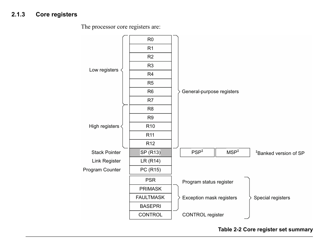
ARM Cortex-M4 has 13 general-purpose registers R0–R12, each 32 bits. Three special registers sit alongside them.
R15 — Program Counter — always holds the address of the next instruction. The MCU increments it by four automatically. When you load an address into R15, the processor starts fetching from there.
R14 — Link Register — stores the return address when a subroutine is called via BL. The subroutine returns by copying LR back into PC. Technically reusable as a general register, but overwriting it before returning is a very common bug.
R13 — Stack Pointer — holds the current top-of-stack address. The stack grows downward. There are two banked versions: MSP (Main Stack Pointer, used in handler mode and privileged thread mode) and PSP (Process Stack Pointer, used by RTOS tasks in unprivileged thread mode). R11 is often used as a frame pointer by compilers.
Program Status Register (PSR)
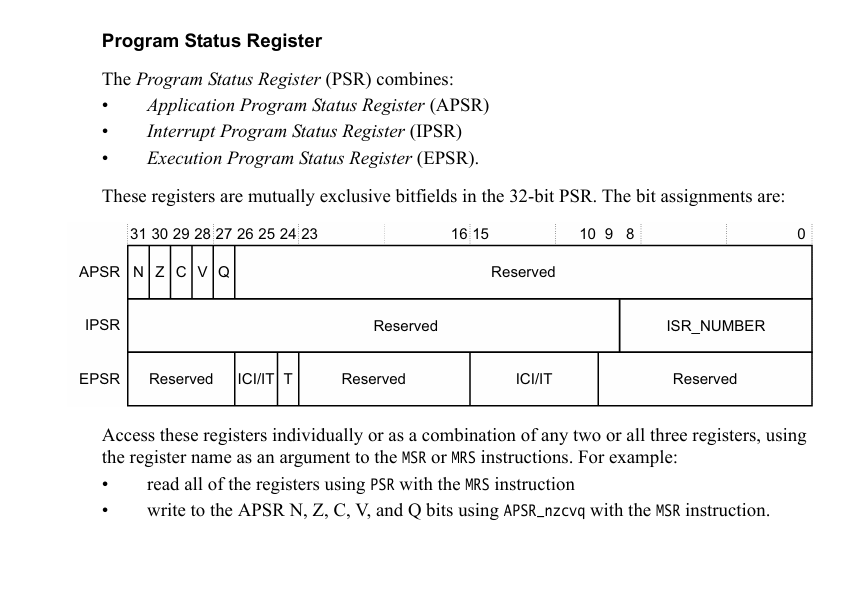
The PSR combines three sub-registers occupying mutually exclusive bit-fields in the same 32-bit word. APSR holds condition flags, IPSR holds the current exception number, EPSR holds execution state (Thumb bit, ICI/IT fields for interruptible load-multiple).
| Flag | Bit | Set when… |
|---|---|---|
| N (Negative) | 31 | Signed result is negative |
| Z (Zero) | 30 | Result equals zero |
| C (Carry) | 29 | Unsigned overflow or last bit shifted out |
| V (Overflow) | 28 | Signed overflow on add/subtract |
| Q (Saturation) | 27 | Saturation occurred (DSP instructions) |
Key instructions for the startup file
ldr and str are the bread and butter of startup code — load from memory into a register, store from a register back to memory. Everything in Reset_Handler before bl main is built on these two.
; ldr rd, [rn, #offset] — load word from (rn + offset) into rd
ldr r0, [r1, #12]     ; C: r0 = *(uint32_t*)(r1 + 12)
ldr r0, [r1]          ; C: r0 = *r1              (offset = 0)

; str rd, [rn] — store rd to address rn
str r0, [r1]          ; C: *r1 = r0

; ldr with = prefix: load any 32-bit constant or symbol address
ldr r0, =0x4005200E   ; r0 = literal 0x4005200E
ldr r0, =_stack_top   ; r0 = address of linker symbol _stack_top
; (assembler places the value in a literal pool, emits a PC-relative ldr)

; strh — store half-word (16-bit). Used for WDOG 16-bit registers.
strh r1, [r0]         ; *(uint16_t*)r0 = (uint16_t)r1

; bl target — branch and link (subroutine call)
bl  main              ; LR = return address, then PC = main

; # vs = syntax
; #imm  — small constant, encoded directly in instruction
mov r2, #0            ; r2 = 0 (fits in 8-bit immediate)
; =val  — any 32-bit value or symbol, via literal pool
ldr r0, =0x40047000   ; r0 = SIM base address
Linker script basics
A linker script describes the physical memory layout of the chip and tells the linker where to place each output section. The memory layout is chip-specific — for the K64F: 1 MB Flash at 0x00000000, 256 KB RAM at 0x1FFF0000. Blue Pill (STM32F103): 64 KB Flash at 0x08000000, 20 KB RAM at 0x20000000.
MEMORY
{
  FLASH (rx)  : ORIGIN = 0x00000000, LENGTH = 1024K
  RAM   (rwx) : ORIGIN = 0x1FFF0000, LENGTH = 256K
}

/* Stack top = end of RAM, 8-byte aligned (AAPCS requirement) */
_stack_top = ORIGIN(RAM) + LENGTH(RAM);  /* = 0x20030000 */

SECTIONS {
  .vectors   → FLASH[0x000]  — SP initial value + handler addresses
  .FlashConfig 0x400 → FLASH  — K64F security block (MUST be here)
  .text      → FLASH         — code + read-only data
  .data      → RAM AT FLASH  — initialized globals (copied at boot)
  .bss       → RAM            — zero-initialized globals
}
.S vs .s: A .S file is processed by the C preprocessor before assembly — it can contain #include, #define, conditional directives. A .s file is pure assembly, no preprocessor. Make sure your Makefile rule matches (%.o: %.s vs %.o: %.S) — this is case-sensitive on Linux/WSL.
— Chapter III: K64F Bare-Metal Bring-Up —
Status summary
✓ Done Working
Boot / Reset_Handler
Watchdog disable
Flash Config Block (0x400)
.data / .bss init
Register headers (MISRA C:2012)
UART0 — 115200 baud
SysTick — 1 ms interrupt
PIT — periodic interrupt
LED / GPIO (PTB22)
→ Up Next TODO
MCG / PLL → 120 MHz
Update CORE_CLOCK_HZ
Interrupt-based UART RX
Context switching (RTOS)
Blue Pill port
NUCLEO-H753ZI port
Boot infrastructure
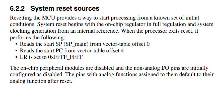
When the chip resets, the CPU reads the initial Stack Pointer from vector-table offset 0 and the Reset_Handler address from offset 4, then jumps there. No C runtime exists yet.
K64F Reference Manual 6.2.2 — System Reset Sources:
; ── 1. Watchdog disable — must be first, before .data copy ──
ldr  r0, =0x4005200E    ; WDOG_UNLOCK register
ldr  r1, =0xC520
strh r1, [r0]           ; unlock key 1
ldr  r1, =0xD928
strh r1, [r0]           ; unlock key 2 (≤20 bus cycles after key 1)
nop
nop
ldr  r0, =0x40052000    ; WDOG_STCTRLH
ldr  r1, =0x01D2        ; WDOGEN=0 (bit0 cleared), rest at reset value
strh r1, [r0]
nop / nop / nop         ; wait ≥1 WDOG_CLK cycle

; ── 2. Copy .data: Flash (LMA) → RAM (VMA) ─────────────────
ldr  r0, =_data_load
ldr  r1, =_data_start
ldr  r2, =_data_end

; ── 3. Zero .bss ────────────────────────────────────────────
ldr  r0, =_bss_start
ldr  r1, =_bss_end
mov  r2, #0

; ── 4. Jump to C ────────────────────────────────────────────
bl   main
The Flash Configuration Block at 0x400 is mandatory. The K64F reads security bytes from here on every boot. Last word must be 0xFFFFFFFE — bit 0 clear means unsecured. If this block is missing or wrong, the chip can lock itself and JTAG becomes unreachable.
Problems & solutions
This section cost me nearly a week and three boards. I am keeping the notes short, but each of these was genuinely a bad day.
1. OpenSDA bootloader recovery
Issue: Application accidentally flashed to the OpenSDA K20 chip, erasing the bootloader. BOOTLOADER drive stopped appearing in Windows.
Solution: Used an FRDM-KL46Z as SWD programmer to reflash Segger J-Link firmware onto the K20 via pyocd on Linux (Windows Storage Service interferes).
pyocd flash -t k20d50m 0226_k20dx128_k64f_0x5000.bin
2. Binary was only 248 bytes
Issue: make succeeded but size showed only 248 bytes. main was not in the binary. I actually thought I had written a very efficient program — a friend noticed something was wrong.
Reason: --gc-sections without an ENTRY point caused main to be discarded as unreferenced.
Solution: Added ENTRY(Reset_Handler) to the top of the linker script.
3. Continuous reset loop — watchdog
Here disable whatchdog on assembly ı implement on startup file but later on c file ı aaded and colling on main file for now ı remove from startup ı wans not sure ı implemented correct ı guess ı calculate address offsets and values wrong on wdog so again ı dont want to damage board :) But later again ı will implement here
And of course from manufacturer startup file also of course can be usable but will not be convenient for MISRA-C issue and ı want to test myself I lost some big money for this but anyway ı am happy for now working .. :)
Issue: After flashing, the board reset every ~2 seconds. HardFault or watchdog timeout. opensda led sometimes error indicate blinks and sometimes directly was red! Specially when you see red it is really dangerous
Reason: K64F watchdog is enabled by default at power-on. Startup jumped to main without disabling it first.
Solution: Added the watchdog unlock + disable sequence as the very first thing in Reset_Handler.
; Reset value: 0x01D3 (WDOGEN=1 — watchdog ON by default)
; We write:    0x01D2 (WDOGEN=0 — only bit 0 changes)
; Unlock sequence must complete within 20 bus cycles:
ldr  r0, =0x4005200E   ; WDOG_UNLOCK
ldr  r1, =0xC520  /  strh r1, [r0]
ldr  r1, =0xD928  /  strh r1, [r0]
nop / nop
ldr  r0, =0x40052000   ; WDOG_STCTRLH
ldr  r1, =0x01D2  /  strh r1, [r0]
nop / nop / nop        ; wait ≥1 WDOG_CLK cycle for WDOGEN bit
4. Missing Flash Configuration Block
This was a nightmare. I do not want to write much about it.
Reason: K64F reads 0x400 on every boot for security settings. Without a .FlashConfig section, this area was uninitialized and the chip entered security mode — JTAG lost.
Solution: Added explicit .FlashConfig at 0x400 in the linker, last word 0xFFFFFFFE.
5. crt0 linker errors
Issue: -specs=nosys.specs / -specs=nano.specs pulled in crt0.o, which expected BSS symbols the linker script did not define.
Solution: Removed those flags, added -nostartfiles.
6. Section name mismatch
Issue: Linker script searched for .isr_vector; startup defined .vectors.
Solution: Synchronized names, added KEEP(*(.vectors)) to prevent --gc-sections from discarding the vector table.
7. gc-sections discarding main
Issue: --gc-sections discarded main as unreferenced.
Solution: Added KEEP(*(.text*)) to the .text section and confirmed ENTRY(Reset_Handler) was present.
Register definitions
I wanted to learn MISRA C:2012 alongside this project, so I tried to apply the rules from the beginning. All MISRA Rule 11.4 violations (integer-to-pointer casts) are documented and centralized in one file — mmio_deviation.h — with a justification comment, so they are easy to audit.
typedef struct {
  volatile uint32_t PDOR;  /* Port Data Output   */
  volatile uint32_t PSOR;  /* Port Set Output    */
  volatile uint32_t PCOR;  /* Port Clear Output  */
  volatile uint32_t PTOR;  /* Port Toggle Output */
  volatile uint32_t PDIR;  /* Port Data Input    */
  volatile uint32_t PDDR;  /* Port Data Direction */
} GPIO_Type;
/* Base addresses — K64 Sub-Family Reference Manual, Chapter 4 */
#define GPIOB_BASE_ADDR   (0x400FF040UL)
#define UART0_BASE_ADDR   (0x4006A000UL)
#define MCG_BASE_ADDR     (0x40064000UL)
#define SYSTICK_BASE_ADDR (0xE000E010UL)

/* MISRA 11.4 deviation — CMSIS-style, isolated to this file */
#define GPIOB   ((GPIO_Type   *)(GPIOB_BASE_ADDR))
#define UART0   ((UART_Type   *)(UART0_BASE_ADDR))
#define MCG     ((MCG_Type    *)(MCG_BASE_ADDR))
#define SYSTICK ((SysTick_Type*)(SYSTICK_BASE_ADDR))
UART0 driver
115200 baud, 8N1. The K64F UART0 has a Baud Rate Fine Adjust (BRFA) field in register C4 — 5 extra bits of fractional precision. Without it, the baud rate error at 115200 from a ~21 MHz clock would be several percent.
/* CORE_CLOCK_HZ = 20971520, baud = 115200 */
sbr_full = (CORE_CLOCK_HZ * 2UL) / baud;
/* ×2 gives 5 extra fractional bits: 20971520×2/115200 = 364 */

sbr  = (uint16_t)(sbr_full >> 5U);    /* = 11  → BDH/BDL */
brfa = (uint8_t) (sbr_full &  0x1F);  /* = 12  → C4      */

UART0->BDH = (sbr >> 8U) & UART_BDH_SBR_MASK;
UART0->BDL = sbr & 0xFFU;
UART0->C4  = brfa;
UART0->C2  = UART_C2_TE_MASK | UART_C2_RE_MASK;
Verified with RealTerm — 115200 8N1. Output stable, no drift observed. A \n → \r\n conversion is applied inside uart0_puts for terminal compatibility.
SysTick timer
Configured to fire an interrupt every 1 ms. Because SysTick's address is architecturally fixed, this driver is portable to any Cortex-M — only CORE_CLOCK_HZ needs to change per board.
/* LOAD = CORE_CLOCK_HZ / 1000 - 1  (counts per 1 ms) */
/* At 20971520 Hz → LOAD = 20970                      */
SYSTICK->LOAD = ((CORE_CLOCK_HZ / 1000UL) - 1UL)
              & SYSTICK_LOAD_RELOAD_MASK;
SYSTICK->VAL  = 0U;
SYSTICK->CTRL = SYSTICK_CTRL_CLKSOURCE_MASK   /* core clock */
              | SYSTICK_CTRL_TICKINT_MASK      /* interrupt  */
              | SYSTICK_CTRL_ENABLE_MASK;      /* start      */

void SysTick_Handler(void) { g_systick_count++; }
Current clock: SysTick is running from the FLL at ~20.97 MHz (FEI mode default). Once MCG switches to 120 MHz, LOAD recalculates automatically from CORE_CLOCK_HZ — no other change needed.
PIT — Periodic Interrupt Timer
INFO : Normally for K64F standart tick ı planned to use PIT for systemTick on my tamga systemtick 24bit PIT 32 bit but whaen ı read abour ROTS's normal systick is standart tick source for all RTOSes... soo probably ı will not use PIT for tick but anywayd as driver ı wrote :)
The K64F PIT module has four independent 32-bit down-counters clocked from the bus clock (core clock / 2). Unlike SysTick, PIT is a vendor peripheral — not architecturally fixed — but it is more flexible: 32-bit range (vs SysTick's 24-bit), four independent channels, and channels can be chained for 64-bit timers.
/* 1. Enable PIT clock gate in SIM */
SIM->SCGC6 |= SIM_SCGC6_PIT_MASK;

/* 2. Enable PIT module (clear MDIS bit in MCR) */
PIT->MCR = 0x00U;

/* 3. Load value = bus_clock_hz / interrupts_per_sec - 1  */
/*    Bus clock ≈ core/2 ≈ 10485760 Hz at FEI mode        */
/*    For 2 Hz (500 ms): 10485760/2 - 1 = 5242879         */
PIT->CHANNEL[0].LDVAL = (BUS_CLOCK_HZ / 2UL) - 1UL;

/* 4. Enable timer and interrupt */
PIT->CHANNEL[0].TCTRL = PIT_TCTRL_TEN_MASK | PIT_TCTRL_TIE_MASK;

void PIT0_IRQHandler(void) {
  PIT->CHANNEL[0].TFLG = PIT_TFLG_TIF_MASK; /* write-1-to-clear */
  /* ... */
}
Critical: The TIF (Timer Interrupt Flag) must be cleared inside the ISR by writing 1 to it — this is a write-1-to-clear register. Forgetting this causes the interrupt to re-fire immediately on return, locking the processor in the ISR.
| Feature | SysTick | PIT |
|---|---|---|
| Counter width | 24-bit | 32-bit (64-bit chained) |
| Architecture | ARM fixed (all Cortex-M) | NXP vendor peripheral |
| Clock source | Core or external ref | Bus clock (core / 2) |
| Channels | 1 | 4 independent |
| Typical use | RTOS tick, 1 ms heartbeat | Longer periods, multiple timers |
LED + GPIO
The red LED on FRDM-K64F is connected to PTB22. Three steps to drive a GPIO output on K64F: enable port clock gate in SIM, set pin mux to GPIO in the PORT module, configure direction in the GPIO module. PORT and GPIO are separate peripherals at separate base addresses — a common source of confusion coming from STM32 where they are more tightly integrated.
/* 1. Enable PORTB clock gate */
SIM->SCGC5 |= SIM_SCGC5_PORTB_MASK;

/* 2. PTB22 → GPIO mode (MUX field = 1) */
PORTB->PCR[22] = PORT_PCR_MUX(1U);

/* 3. Set as output */
GPIOB->PDDR |= (1UL << 22U);

/* 4. Toggle in while(1) */
GPIOB->PTOR = (1UL << 22U);
INFO: K64F has active-low led pins so when you write 0 it will shine !!! Plese check schematic on sources ı put already pdf for K64F
— Chapter IV: What's Next —
Up next: MCG clock — 120 MHz
The K64F is currently running at ~20.97 MHz in FEI mode (FLL driven by the internal reference oscillator). The chip's maximum is 120 MHz, which requires the PLL via the MCG state machine. You cannot jump directly to PLL output — you must step through intermediate states in order.
FEI  ~21 MHz    ← currently here (FLL, internal RC)
 ↓
FBE             ← select 50 MHz external reference (EXTAL0 — PHY REF_CLK)
                   MCG_C2: RANGE0=1, EREFS0=1 / MCG_C1: CLKS=10
                   wait: OSCINIT0=1, IREFST=0, CLKST=10
 ↓
PBE             ← enable PLL (MCG_C5: PRDIV0, MCG_C6: VDIV0 + PLLS=1)
                   wait: PLLST=1, LOCK0=1
 ↓
PEE  120 MHz  ← switch core to PLL (MCG_C1: CLKS=00)
                   wait: CLKST=11
/* EXTAL0 = 50 MHz (Ethernet PHY REF_CLK on FRDM-K64F)         */
/* PLL reference must be in the 2–4 MHz window                  */
/* real_divider = PRDIV0_field + 1  (field range 0..24)         */
/* real_multiplier = VDIV0_field + 24  (field range 0..31)      */
/* PLLCLK = (EXTAL0 / real_divider) × real_multiplier           */

real_divider   = 20          → PRDIV0 field = 19
PLL_ref        = 50/20       = 2.5 MHz  ✓ within 2–4 MHz window
real_multiplier = 48         → VDIV0 field  = 24
PLLCLK         = 2.5 × 48   = 120 MHz  ✓

/* Other valid outputs from 50 MHz: */
/* 96 MHz:  50/25=2.0 × 48 = 96  (PRDIV0=24, VDIV0=24) */
/* 48 MHz:  50/25=2.0 × 24 = 48  (PRDIV0=24, VDIV0=0)  */
/* 110 MHz: 50/25=2.0 × 55 = 110 (PRDIV0=24, VDIV0=31) */
The init_mcg(uint32_t target_mhz) function searches all valid (PRDIV0, VDIV0) pairs at runtime, so init_mcg(48), init_mcg(96), and init_mcg(120) all work without manually changing any constants.
/* mcg.h — board-specific oscillator constant */
#define EXTAL0_HZ (50000000UL)

/* MK64F12REGS.h */
/* before: */ #define CORE_CLOCK_HZ (20971520UL)
/* after:  */ #define CORE_CLOCK_HZ (120000000UL)

/* SysTick LOAD and UART baud rate both derive from          */
/* CORE_CLOCK_HZ at compile time — no other changes needed.  */
References
Everything above can be verified against these primary sources. When in doubt, read the spec — not a blog post. Including this one.
ARM architecture
- ARMv7-M Architecture Reference Manual -- PDF --
- ARMv7-M Architecture Reference Manual
- Cortex-M4 Technical Reference Manual
- MISRA-C
NXP K64F
- K64 Sub-Family Reference Manual (K64P144M120SF5RM)
- FRDM-K64F Product Page — NXP
- NXP FRDM-K64F Schematic File